Tutorial 4 of 6
Transistors, op-amps and the 555
Intermediate 15 min
Switch an LED with an NPN transistor, build inverting and non-inverting amplifiers, and make a 555 blink. Each one is checked against the textbook formula.
Ohmforge's semiconductor models are simplified but physical: Ebers–Moll BJTs with Early effect, level-1 MOSFETs, Shockley diodes with series resistance, a single-pole op-amp with rails, and a behavioural 555. Every circuit below is a template, so you can open it and follow along.
1. The transistor as a switch
Open Transistor switch. SW1 feeds the base of Q1 (2N3904) through R1 = 10 kΩ. The collector drives a green LED through R2 = 470 Ω from 9 V. Press Run (F5, DC operating point) and open Results:
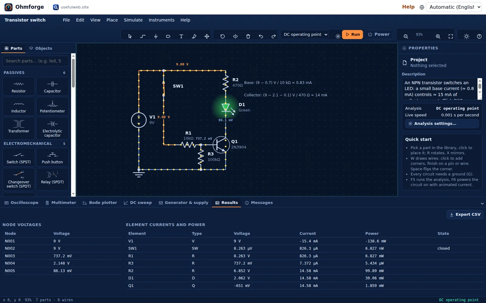
| Quantity | Hand calculation | Ohmforge |
|---|---|---|
| Base current | (9 V − 0.7 V) / 10 kΩ ≈ 0.83 mA | 826.3 µA |
| Base voltage | ≈ 0.7 V | 737.2 mV |
| Collector current | (9 V − 2.1 V − 0.1 V) / 470 Ω ≈ 14 mA | 14.58 mA |
| V(CE) | "saturated", ≈ 0.1 V | 86.1 mV |
The transistor's current gain (β) is about 400, so 0.83 mA of base current could carry over 300 mA. The LED circuit only allows about 15 mA, so the transistor is saturated: fully on, with less than 0.1 V across it. Designers aim for exactly this, a "forced β" of 15 mA / 0.83 mA ≈ 18, far below the real β, so the switch stays saturated even with a weak transistor.
Now press Power (F6) and click SW1. The LED goes off and the base current drops to zero. The current dots on the schematic show the small base loop and the larger collector loop.
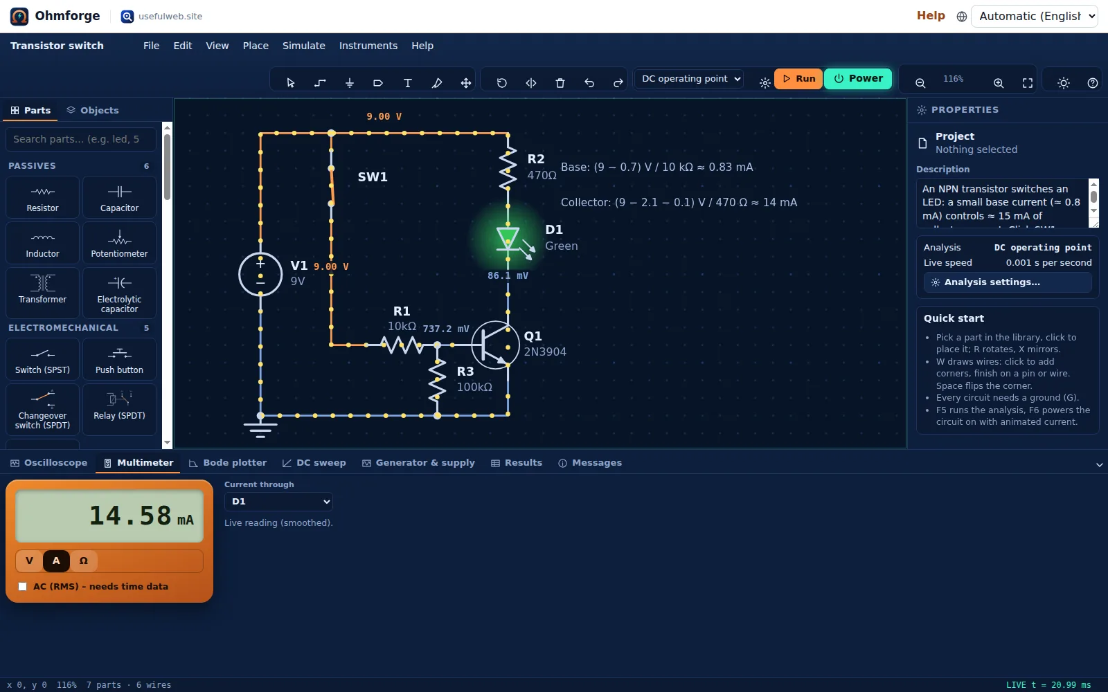
Try it: raise R1 to 470k. The base current falls to 17.7 µA, and the collector current drops to 4.67 mA (β × I_B) instead of being limited by the LED. V(CE) rises to about 4.9 V and the LED dims. The transistor has left saturation and now works in its active region, as an amplifier rather than a switch.
The MOSFET PWM dimmer template does the same job with a logic-level N-MOSFET (IRLZ44N) switching a 12 V lamp at 1 kHz and 25 % duty. Its transient tool measures the gate drive at duty: 0.25 and the drain at duty: 0.75: the drain is low while the gate is high. The H-bridge template combines four BJTs to drive a load in both directions.
2. Op-amps: the golden rules, then reality
Inverting amplifier (ideal)
Inverting amplifier (ideal op-amp) uses R1 = 1 kΩ and R2 = 10 kΩ, so the gain is −R2/R1 = −10. A 0.5 V, 1 kHz sine goes in. Run the transient (F5) and the scope shows:
- IN: 1 V pp, OUT: 10 V pp, inverted, at 1 kHz,
- the inverting input stays at practically 0 V (a "virtual ground").
The ideal op-amp has a fixed open-loop gain of 1 000 000 and no supply pins. It reproduces the textbook rules exactly.
Non-inverting amplifier (real model)
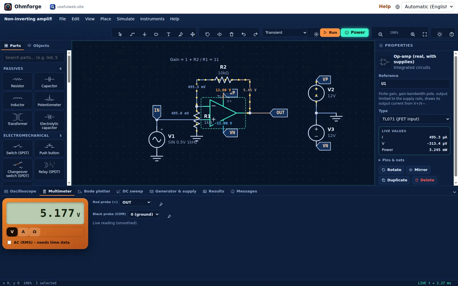
Non-inverting amplifier (TL071, ±12 V) places the Op-amp (real, with supplies) part. It has a finite open-loop gain (200 k), a 3 MHz gain-bandwidth product, and an output that can't come closer than 1.5 V to either rail. Its gain is 1 + R2/R1 = 11.
Things to try:
- Click U1. The inspector shows the model preset (TL071) and its parameters. While the circuit runs, Live values show the op-amp's output current and power (a few mW).
- Raise V1's amplitude to 2 V. 2 V × 11 = 22 V doesn't fit inside ±12 V, so the output clips flat at ±10.45 V.
- Switch to the Bode plotter and sweep. The −3 dB corner sits at GBW / 11 ≈ 271 kHz (see tutorial 3).
3. The 555 astable
Open 555 astable LED blinker. The 555 runs from a 9 V battery with RA = R1 = 10 kΩ, RB = R2 = 68 kΩ and C = C1 = 10 µF.
The textbook formulas give:
- f = 1.44 / ((RA + 2·RB) · C) = 1.44 / (146 kΩ · 10 µF) ≈ 0.986 Hz
- duty = (RA + RB) / (RA + 2·RB) = 78 / 146 ≈ 53.4 %
Press Power. The blinker runs in real time (its live speed is 1 s per second), so the LED blinks about once a second. Open the Oscilloscope with OUT on CH1 and CAP on CH2:
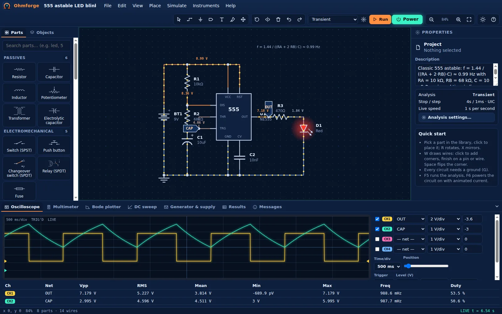
The capacitor charges and discharges between ⅓ and ⅔ of the supply (3 V and 6 V). The output switches at each threshold. The transient tool measures this template at frequency: 0.9877 Hz and duty: 0.533, within 0.2 % of the formula.
Why does the template set UIC ("Start from initial conditions") in its analysis settings? An astable has no stable DC state. If you run a DC operating point on it, Ohmforge says so in Messages:
No stable DC state: U1 keep switching (the circuit oscillates, e.g. a 555 astable). The operating point shown is one of the states; use a transient analysis.
With UIC the transient run skips the operating point. The capacitors start empty and the oscillation builds up by itself, just like on the bench.
Change the timing
- Change C1 to
22u: the blinking slows to 0.449 Hz (the formula gives 0.448 Hz). - Make R2 smaller: the frequency rises and the duty cycle moves towards 100 %, because the high time also includes RA. For duty cycles below 50 %, add a diode across RB.
Where the models stop
- The BJT and MOSFET models have no self-heating, breakdown or temperature dependence. Ratings (maximum collector/drain current, maximum power) are only checked, and a violation shows up as a stress warning.
- The 555 is behavioural: comparators, flip-flop and discharge transistor are ideal. Its output stage drops about 1.7 V when high, so OUT peaks at 7.18 V on the 9 V battery.
- The real op-amp has one pole and no slew-rate limit, so very fast large-signal edges look better than on a real TL071.